|
ADI-8 PRO Inside
ADI-8 PRO architecture, technical specifications and test results The ADI-8 PRO is a reference-quality, 8-channel A/D and D/A converter. This Tech Info is aimed at technically-minded readers, and covers details which were not mentioned in either the general product description or the User's Guide. Overview The ADI-8 PRO internal structure can be divided into 4 distinct functional blocks:
This photo shows the internal structure of an ADI-8 PRO, after having opened the case. As the block diagram clearly shows, the ADI-8 PRO can be routed internally in many ways which, in addition to its function as A/D-D/A converter, allows it to be used as a format converter, distributor or splitter.
Analogue to Digital Physical access to the analogue inputs is either via 1/4"
stereo jack socket or 25-pin D-type connector conforming to the Tascam DAxx
analogue I/O pinout. These recorders are very common, so a suitable multicore
cable (e.g. for connecting directly to mixing consoles or to XLR) should
be relatively easy to find. The entire input stage - from the sockets to
the converter chip's internal input - is fully symmetrical. This is a special
servo-balanced input circuit: if the signal
at the input is unbalanced, input gain is automatically adjusted by +6 dB.
Otherwise input sensitivity for an unbalanced signal would have been lower
than for a balanced one.
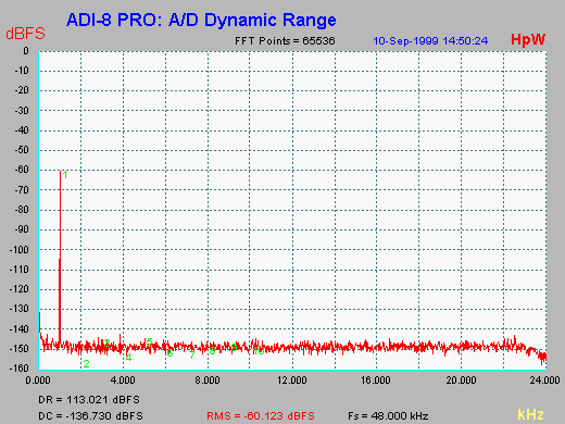
Low noise JRC4580 op-amps are used throughout. This type can be found in countless appliances - it is an unbeatable combination of low noise, low output impedance and low price. However, simply sticking 4580s into your devices will not guarantee you the best possible technical spec - the surrounding circuitry has to be up to scratch as well. We decided on AKM5392 as the A/D converters. These high-end components are relatively expensive, but on the other hand they are almost unbeatable quality. The combination of our special fully-symmetrical input stage with these converters is the main reason for the exceptional 112 dB SNR RMS unweighted (115 dBA), as well as extremely low distortion (THD), below -110 dB (0.0003 %.) Remember that these are not just phantom values copied from the component manufacturer's' spec-sheets - they are the results of real tests on a complete product in a standard environment.
Things started getting really interesting when we checked
the ADI-8 PRO for distortion caused by the A/D converters. Our low-jitter
design, the fully symmetrical input stage and the excellent AKM converters
caused an unusual problem: Any distortion we could measure came from whatever
signal generator we were using for the test - we detected no distortion
attributable to the ADI-8 PRO's input. Did we go out and buy another expensive
audio analyzer just for this test? No, we did something that many people
in this business would normally avoid like the plague: we used the ADI-8
PRO's own analogue output as the signal source. Normally, this would completely
ruin any chance of good results for the A/D converter - but the ADI-8 PRO
is not a normal machine...see below for more about this incredibly high-quality
D/A conversion.
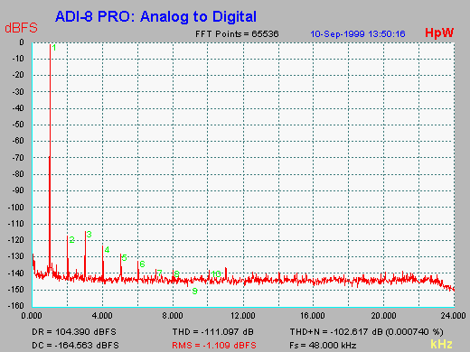
Note that the quality of the A/D conversion on its own would be about 3 dB better than this combined A/D-D/A test. The THD+N should therefore be about -105 dB, SNR should be - assuming a perfect signal generator - much lower (about 5 dB), because the noise component from the D/A converter is more evident here. Take another look at Fig. 2, where a very low-noise signal was used. Jitter Experts will have recognized it immediately: the small
bell-shaped curve at the base of the 1 kHz sine is caused by jitter. Usually
nothing special - but in this case it is doubly so!
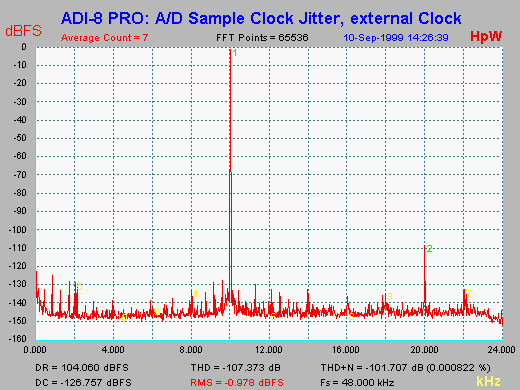
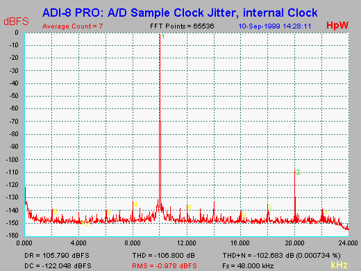
With interface jitter, we are usually talking in terms of nanoseconds. Sample clock jitter is much shorter still - the ADI-8 PRO attains spectacular values of under 20 ps (picoseconds, 10 to the power of minus 12.) However, jitter naturally depends on the clock mode being used. Fig. 4 illustrates a worst-case situation, the ADI-8 A/D set to INP (slave clock mode), so it is being clocked by an external device (in this case a DIGI96/8.)
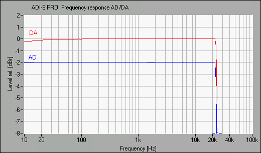
Looking at these two results, you might be tempted to run only INT/INT in future. But to put things in perspective: individual peaks at around -125 dBFS (see frequencies below 2 kHz) are completely insignificant when the signal itself is 120 dB higher. The dimensions become clearer when you look at the values for THD+N and DR (see fig. 4 and fig. 5) - they are almost identical. In principle you could get a cleaner result (even damping the peaks below 2 kHz) by using a particularly slow i.e. highly filtered and/or quarz-based PLL. We have very good reason for not even trying these out. Our bitclock PLL requires a minimum rate to track ADAT XT Varipitch consistently, i.e. without any dropouts. Nevertheless, it still has excellent jitter-damping, beating wordclock-based PLLs by far. Quarz-based or highly filtered PLLs react adversely to rapid changes in sample frequency, causing dropouts (clicks/mute) - several samples will be read falsely before the PLL adjusts to the new sample frequency. This is much more of a problem for the 8-channel ADAT format than for the 2-channel S/PDIF or AES/EBU formats. The frequency response of ADI-8 PRO's analogue input is flawless (see below.) However, thanks to multiple oversampling, only very poorly designed pieces of equipment would exhibit any significant deviation these days. In other words, frequency response curves (as seen in audio journals) of any modern professional equipment - not only ours - are and should be absolutely flat. No Dither? No Dither! Dither is not a simple exercise in a device which has been realized using only FPGA. Besides, in certain cases it can be dispensed with altogether. If you would like to know more about this view (which some might consider provocative), please read the Tech Info Remarks about the Need for Dither. Digital to Analogue In the first ADI-8 PRO version we used the Analog Devices
AD1855 chip as D/A converter, because this was the first DAC to achieve
110 dB dynamic range without resorting to muting to improve S/N ratio. At
the same time, the AD1855 is relatively cheap, which is especially important
for multichannel converters such as the ADI-8 PRO, with its 4 converter
chips.
Admittedly, we used a particularly good D/A channel during this test. Analog Devices specify for their AD1852 a THD of 'only' < -104 dB, but in reality values for individual components vary between 105 and 112 dB. Therefore we declared a value of <-105 in our ADI-8 PRO spec. As far as noise from the ADI-8 PRO D/A is concerned, results from a Neutrik A2D ranged from 106 to 110 dB RMS unweighted (depending on the clock configuration and source), or 108 to 112 dBA. Like the inputs, the ADI-8 PRO revision 2 analogue outputs
also have a 3-stage gain switch. The same rule also applies here: Intelligently
designed gain compensation is the only practical way to ensure maximum performance.
The ADI-8 PRO output stage, with its electronic switching and optimized
low-noise output circuitry, reaches the maximum SNR of 110 dB RMS unweighted
at +4 dBu and Hi Gain. In the -10 dBV position, SNR is still 104 dB RMS
unweighted. The difference is no reason for concern here - 104 dB still
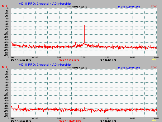
means that the ADI-8 PRO is reference-quality. Crosstalk When audio signals are as clean as this, crosstalk should
also be extremely low. Crosstalk can be measured by feeding one channel
with a 1 kHz sine at the highest level possible, and then measuring the
RMS level in a neighboring channel. The 1 kHz crosstalk signal is isolated
using a narrow bandpass filter, removing noise before the level is measured
(because crosstalk can be well below the noise floor in a well-designed
system.) For the same reason, the input of the channel being measured is
also grounded.
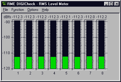
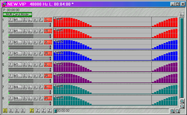
TDIF The ADI-8 PRO's TDIF connections support 24-bit audio and emphasis (since revision 2), and run without any word clock problems of any kind. You are free to use word clock of course, but in most cases this is not necessary. We have also dispensed with jumpers and other configuration aids for different operating modes, as they are completely unnecessary in a well-designed TDIF interface. There is only one restriction to the above rule (caused by the necessity to support the DA-88/38): If the recorder is the slave, the ADI-8 PRO's word clock output MUST be connected to the recorder's word clock input. The other way around no word clock connection is needed - despite what some manufacturer's (and therefore many users) may claim. ADAT optical The ADAT optical connections in the ADI-8 PRO support 24-bit audio, and run without any word clock problems of any kind. Of course you are free to use word clock - but in most cases this is not necessary. The ADI-8 PRO always uses RME's bitclock PLL (already in its second generation, with improved HF noise suppression), whether it is synchronized via Optical In or via word clock. Thanks to the high resolution, this remarkable circuit is capable of following the entire range of an ADAT recorder's Varipitch without losing a single sample. Compare this with the much coarser wordclock PLL, where any rapid changes in sample frequency can cause several false reads, before the next impulse finally arrives, letting the PLL track the current sample frequency. This behavior leads to dropouts and clicks. So as long as you use an ADI-8 PRO, anything goes. With other brands it's a case of 'suck it and see'... SyncAlign SyncAlign embraces a whole bunch of techniques to guarantee absolutely perfect timing and no channel problems. SyncAlign was first realized in the DIGI96 series, and of course we have implemented it in the ADI-8 PRO as well. The ADI-8 PRO will NEVER mix up channels, no matter which clock mode is being used. SyncAlign also regulates synchronization between channels (the screenshot below illustrates the sample-sync capability - it shows individual samples of a single 1 kHz sine-wave sent to all channels.) Even when several ADI-8 PROs are synchronized via word clock, the converted signal always appears absolutely in sync across all digital outputs.
Clock Control The various functions in the ADI-8 PRO are all handled
by an FPGA (field programmable gate array) control unit. If you don't know
what an FPGA is, imagine it to be a kind of fixed-program microcontroller.
This chip controls the sample frequency
of both A/D and D/A, their switching, evaluation and display of clock synchronism
(SyncCheck), evaluation and display of analogue levels, and much more. It
is also responsible for managing audio data, e.g. format conversion, splitting
and mixing, as well as audio buffering (see the section 'Delay' below.) Delay Any digital device causes a delay between input and output. As the ADI-8 PRO does not contain any DSPs, there are only two relevant delays:
The Power Supply When designing a power supply for a combined A/D-D/A device,
you have to bear a lot of criteria in mind. While looking for the best solution,
we soon decided on a switch-mode PSU. The first advantage that springs to
mind is that they automatically accept 100 to 240V (the international range
of mains power.) This is very important from the manufacturer's point of
view - we only need to build a single model for the entire international
market. Remarks about the Tests RME carries out all tests using professional measuring instruments, adhering to standardized metrological guidelines. We consider it important to arrive at real results under real test conditions. Some of the competition prefers to copy their data straight from chip-manufacturer's' spec-sheets. Such fantasy-results are not only deceitful, but are also impossible to reach - for two reasons: Firstly, they don't take into account all the other active electronic components in the finished product. Secondly, it is common knowledge that quite a few chip specs themselves are 'ultimate goal' values, only reached after several revisions - if at all. Double-checking these results by plowing through magazines looking for RME product tests is unnecessary - these are real tests and real results. We use the Neutrik A2D and its accompanying software AS04 (www.neutrik.com) for our analogue and digital measurements. This yields (among other things) RMS unweighted or weighted results according to defined industrial standards, for levels, distortion and noise, as well as sweeps for nearly all parameters (see blurb about frequency response.) The A2D is a must for hardware developers thanks to its simple operation, high-precision results, and its connectivity. For purely digital measurements, we use a reference-level
Windows program called
HpW Works. This software has a very high resolution and delivers unbeatably
accurate results. Apart from the FFT analyses mentioned above, it can also
be used to generate highly accurate digital signals.
Copyright © RME, Matthias Carstens, 1999. |
|||||||||||||||||||||||||||||||||||||||||||||||||||||||
Copyright © 2002 RME. All rights reserved.
RME is a registered trademark. |
|||||||||||||||||||||||||||||||||||||||||||||||||||||||