FAQ Topics
FAQ Topics
Modification of the HDSP PCI card
The Hammerfall DSP system with PCI card does not work correctly on a few computers. Unsuccessful boot initialization shows the following symptoms:
- The PCI card is not found by the system during boot-up. It does not appear as Multimedia Device in the list of PCI devices, nor in Windows' device manager.
- The hammer symbol does not show up in the Systray of Windows 2000/XP. The Settings dialog is not being loaded, because the card (the HDSP system) is not present. The mixer symbol (TotalMix) shows up in any case.
- The Settings dialog remains empty (Mac OS) or shows 'Error' (Windows 98).
- The system does not work (ASIO error etc.).
In all cases it is the same error. Directly after switching on the computer the power supply ramps up its output voltages. But already during the ramp up several components begin to draw high currents and cause voltage fluctuations. This can cause the FPGA on the HDSP-PCI card to hang. As a consequence, the card is virtually dead and cannot be detected by the computer nor initialized.
Exchanging the computer's power supply into a stronger one of a known brand solved the problem for many customers. RME have taken care to make the HDSP PCI card safe against voltage drops during boot-up. The modification published 06/26/02 solved the problem for most affected customers. Finally a computer showing the error reached our lab. The problem was finally identified and fixed. The new modification can be done with boards of all revisions. The current revision 1.5 now ships in a modified version.
Please note that this modification may only be done by qualified service personnel. Improper handling of the PCI card causes loss of warranty and there will be repair or exchange costs. The normal procedure in case of boot/initialization problems is exchanging the PCI card via your retailer and/or distributor against a modified card.
We are giving this information here, because we are aware of the fact that exchanging the PCI cards will need a certain time in some cases, whereas any competent technician can do the modification within less than 5 minutes.
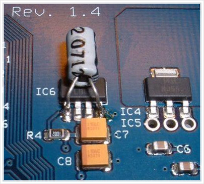
Modification of Revision 1.3 and 1.4

A modification of revision 1.3 and 1.4 is very simple. Just solder a capacitor 4.7 µF, at least 10 Volt, to pin 1 and 4 of the voltage regulator IC6. In case an electrolytic type is used: the negative pin must be on the right side, at pin 4, see picture to the left.

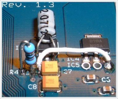
In case the modification from 06/26/02 has been applied and did not fix the problem, proceed as follows:
Remove only the wire (or 0 Ohm resistor) which replaced R4, and solder the original R4 (10 kOhm) back on its pads. Now add the 4.7 µF capacitor as described above. Do not undo the other modifications (removal of top layer pad, connection of left side of C7 with the right pin of IC4 by means of an insulated wire).
Modification of Revision 1.5
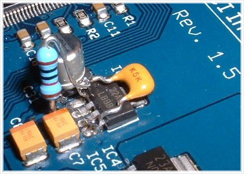
As revision 1.5 no longer includes a R4, the resistor has to be added and inserted. This is done by unsoldering and bending pin 1 of IC6 high. Then a resistor 10 kOhm is soldered to the left side of C7 and the upwards bended pin, see picture to the left. Next a capacitor 4.7 µF, at least 10 Volt, is soldered to pin 1 and 4 of the voltage regulator IC6. In case an electrolytic type is used: the negative pin must be on the right side, at pin 4.

Technical note: This modification causes the FPGA to be powered with a slight delay, when the computer's power supply generates a stable output voltage.

